X-Microwave Design System
I came across an awesome system for rapid prototyping RF and Microwave solutions
by connecting individual components on small PCBs, just like LEGO.
This Modular building block system for RF and microwave design of prototypes is in my opinion a very clever way of building RF
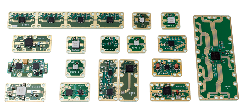
circuits. On their website the sell almost every
available modern RF IC or passive network in a form of a rectangle PCBs.
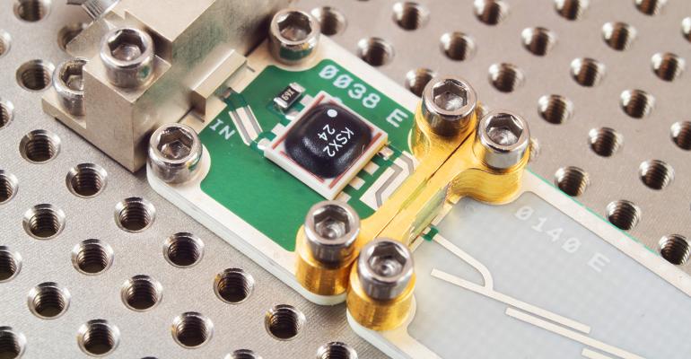
The whole system is well polished and every part has some sort of improvement. For example the boards interconnection has a ground cutout, probably for better impedance matching. The connection is done (according to their patent) with a small piece with diamond particles that improve contact. That’s why they claim that this system can be used up to ~67 GHz.
Of course this performance comes at a price.
My own design
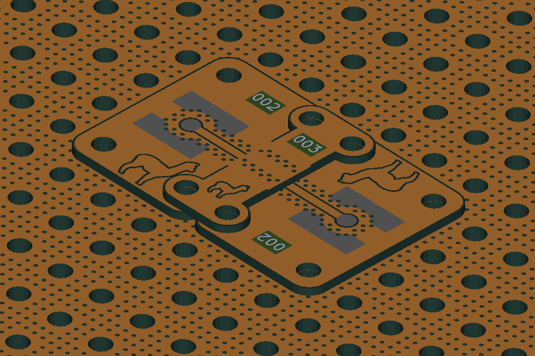
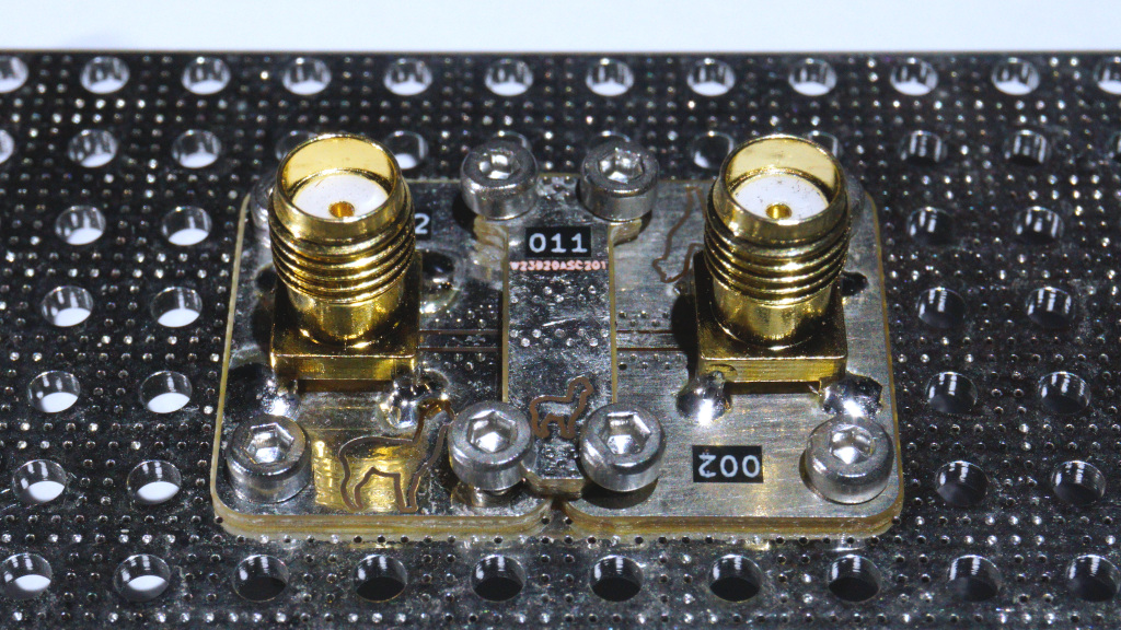
I liked this idea so much that I wanted to check how bad will standard FR4 boards perform if someone would make a system like this one. But without all those whistles.
So I made ten different designs inspired by that system. Ordered it on PcbWay.
And when will it arrive I will test it with my VNA.
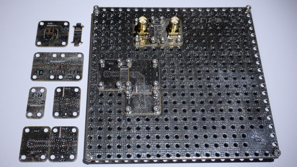
After some time the boards arrived in decent quality. I soldered SMA connectors to two boards designed for them and screwed them to the PCB base, together with a small interconnecting PCB.
I tried to follow X Microwave design but my idea had some problems. The small board with the number 011 that was designed to connect other boards didn’t make good contact after mounted with screws. It just bulged up and the center signal trace didn’t touched the traces on the other PCBs. But after adding a small amount of solder to the trace it started to work.
Measurements
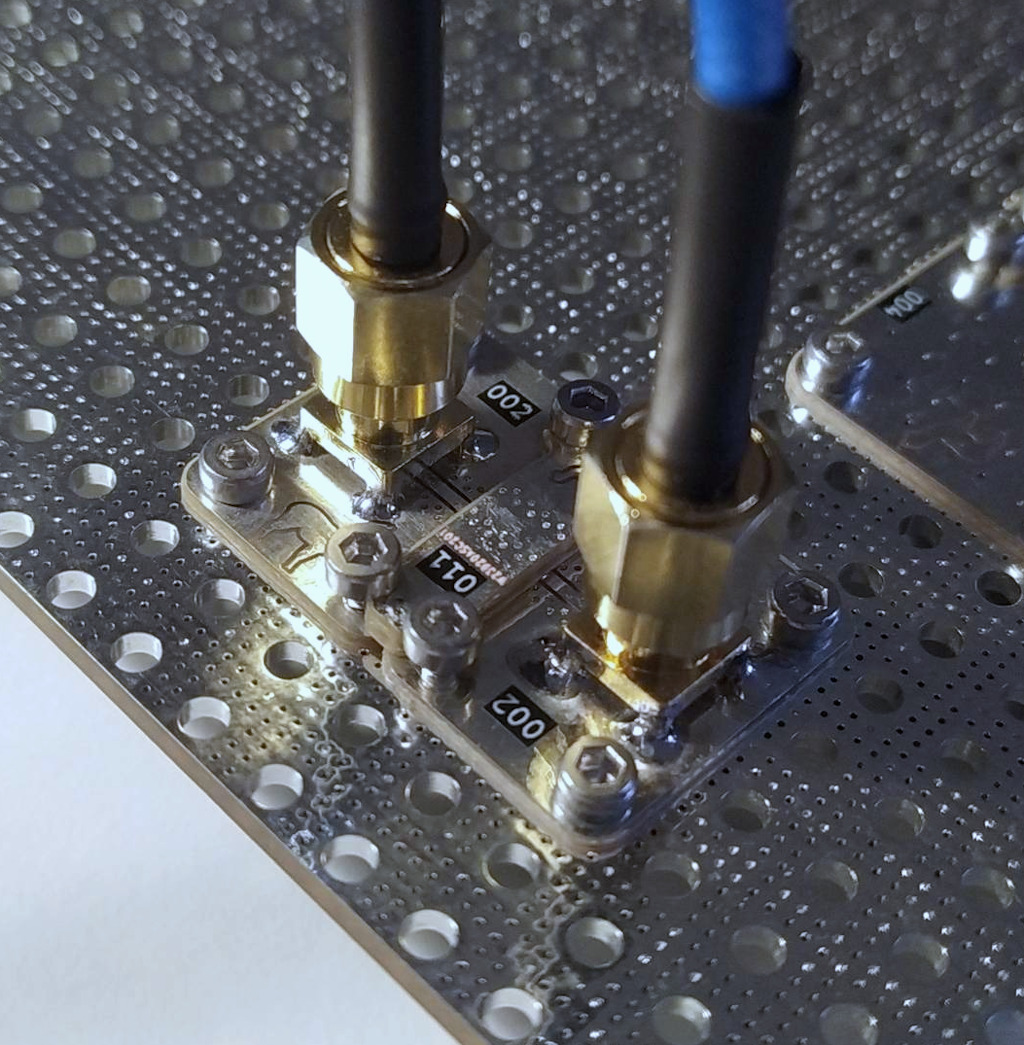
Measurements of two connected SMA adapters done on nanoVNA.
S11 50 Ohm termination
 S11 50 Ohm termination by Port 2 of nanoVNA
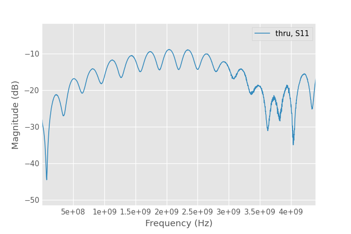
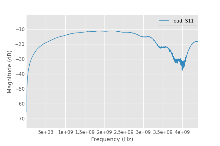
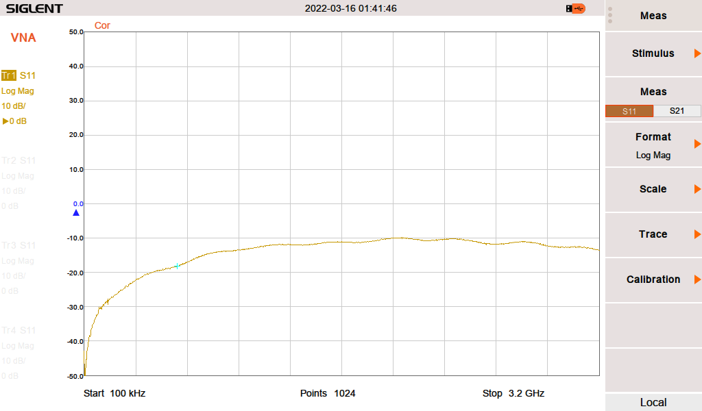
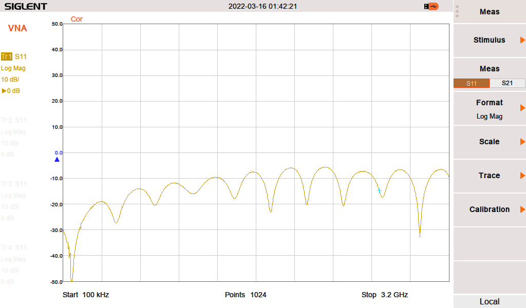
Measurements of two connected SMA adapters done on better VNA.
S11 50 Ohm termination
 S11 50 Ohm termination by Port 2 of VNA
 S21
S21
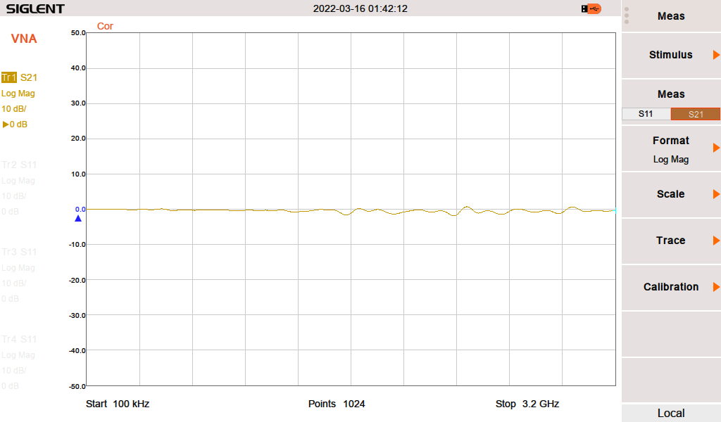
I wasn’t excepting much after 0,8 mm FR4 PCB but it is usable up to 1,5 GHz. The board to board connection is working and everything is pretty durable.
I plan to design modules for a FM receiver. If it works, I’ll share it on github.
You can find all files under this github repository.